(China (Mainland))


Product Summary
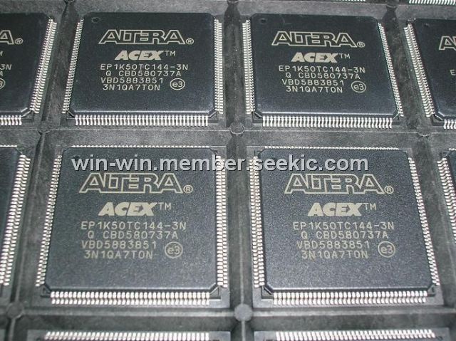
The EP1K50TC144-3N is a 1K Programmable Logic Device providing a die-efficient, low-cost architecture by combining look-up table (LUT) architecture with EABs. LUT-based logic provides optimized performance and efficiency for data-path, register intensive, mathematical, or digital signal processing (DSP) designs, while EABs implement RAM, ROM, dual-port RAM, or first-in first-out (FIFO) functions. These elements make the EP1K50TC144-3N suitable for complex logic functions and memory functions such as digital signal processing, wide data-path manipulation, data transformation and microcontrollers, as required in high-performance communications applications. Based on reconfigurable CMOS SRAM elements, the EP1K50TC144-3N incorporates all features necessary to implement common gate array megafunctions, along with a high pin count to enable an effective interface with system components. The advanced process and the low voltage requirement of the 2.5-V core allow the EP1K50TC144-3N to meet the requirements of low-cost, high-volume applications ranging from DSL modems to low-cost switches.
Parametrics
EP1K50TC144-3N absolute maximum ratings: (1)VCCINT, Supply voltage With respect to ground: –0.5 to 3.6 V; (2)VCCIO: –0.5 to 4.6 V; (3)VI, DC input voltage: –2.0 to 5.75 V; (4)IOUT, DC output current, per pin: –25 to 25 mA; (5)TSTG, Storage temperature No bias: –65 to 150℃; (6)TAMB, Ambient temperature Under bias: –65 to 135℃; (7)TJ, Junction temperature: 135℃.
Features
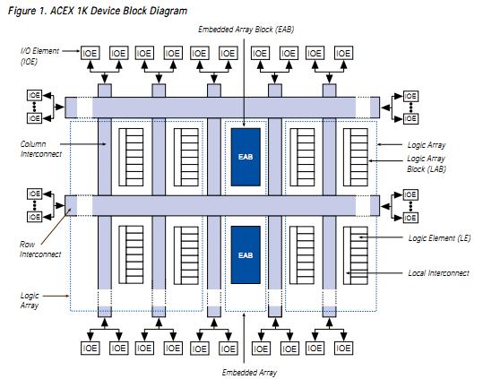
EP1K50TC144-3N features: (1)Programmable logic devices (PLDs), providing low cost system-on-a-programmable-chip (SOPC) integration in a single device: Enhanced embedded array for implementing megafunctions, such as efficient memory and specialized logic functions; Dual-port capability with up to 16-bit width per embedded array block (EAB); Logic array for general logic functions; (2)High density: 10,000 to 100,000 typical gates (see Table 1); Up to 49,152 RAM bits (4,096 bits per EAB, all of which can be used without reducing logic capacity); (3)Cost-efficient programmable architecture for high-volume applications: Cost-optimized process; Low cost solution for high-performance communications applications; (4)MultiVoltTM I/O pins can drive or be driven by 2.5-V, 3.3-V, or 5.0-V devices; (5)Low power consumption; (6)Bidirectional I/O performance (setup time [tSU] and clock-to-output delay [tCO]) up to 250 MHz; (7)Fully compliant with the peripheral component interconnect Special Interest Group (PCI SIG) PCI Local Bus Specification, Revision 2.2 for 3.3-V operation at 33 MHz or 66 MHz; (8)Extended temperature range.
Diagrams
| Image | Part No | Mfg | Description |  |
Pricing (USD) |
Quantity | ||||||
|---|---|---|---|---|---|---|---|---|---|---|---|---|
 |
 EP1K50TC144-3N |
|
IC ACEX 1K FPGA 50K 144-TQFP |
Data Sheet |
|
|
||||||
| Image | Part No | Mfg | Description | |
Pricing (USD) |
Quantity | ||||||
 |
EP1K100FC256-1 |
|
IC ACEX 1K FPGA 100K 256-FBGA |
Data Sheet |
|
|
||||||
|
EP1K100FC256-1N |
|
IC ACEX 1K FPGA 100K 256-FBGA |
Data Sheet |
|
|
||||||
|
EP1K100FC256-2 |
|
IC ACEX 1K FPGA 100K 256-FBGA |
Data Sheet |
|
|
||||||
|
EP1K100FC256-2N |
|
IC ACEX 1K FPGA 100K 256-FBGA |
Data Sheet |
|
|
||||||
|
EP1K100FC256-3 |
|
IC ACEX 1K FPGA 100K 256-FBGA |
Data Sheet |
|
|
||||||
|
EP1K100FC256-3N |
|
IC ACEX 1K FPGA 100K 256-FBGA |
Data Sheet |
|
|
||||||